Companies that make the tools for the semiconductor companies, including Applied Materials, ASML and Taiwan Semiconductor Manufacturing, are heading for a golden period
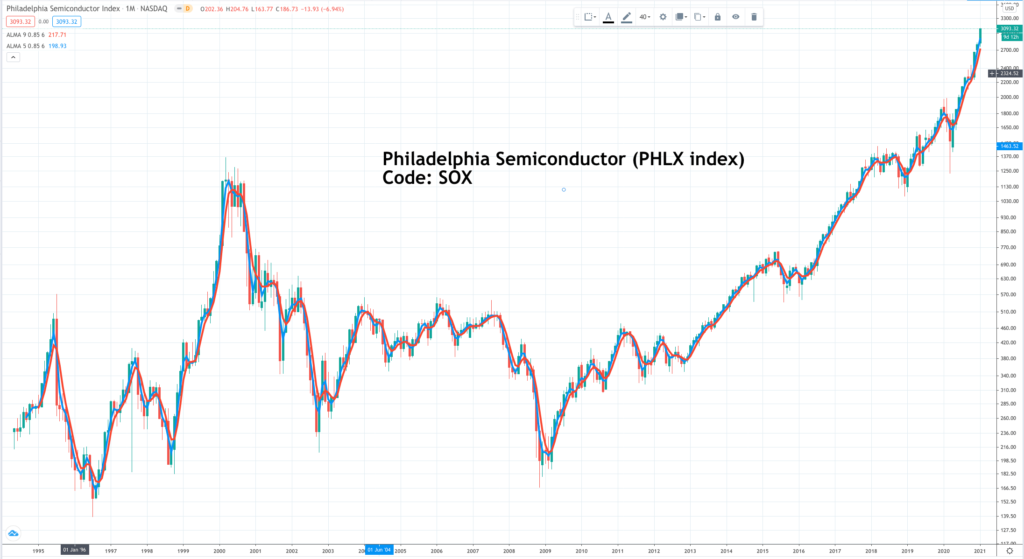
Below I look not at the chip designers like Nvidia and Advanced Micro Devices but at the companies, which make the tools and provide the raw materials of this industry. Think of them as making the shovels for a gold mining boom and you can see why they are so well placed. They are also fabulous businesses, fully deserving of their success. The three I look at below, all in the QV for Shares portfolio but still placed for even greater gains in the future, are Applied Materials, ASML, based in the Netherlands and Taiwan Semiconductor Manufacturing (TSM), based in Taiwan and so important to that country it almost is Taiwan.
Applied Materials AMAT Buy @ $105 MV: $99.9bn Employees: 24,000 Next figures: 18 February Times recommended: 2 First recommended: $82 Last recommended: $89
Applied Materials describes itself as ‘the global leader in materials engineering’ that straightaway sounds exciting but there is something else going on, which suggests that AMAT and the semiconductor industry as a whole, is at an inflexion point, which is going to drive strong growth in the future.
Going into slightly more detail about what they do: “Applied Materials is the leader in materials engineering solutions used to produce virtually every new chip and advanced display in the world. Our expertise in modifying materials at atomic levels and on an industrial scale enables customers to transform possibilities into reality.”
Here we need a little history. For decades the semiconductor industry and technology generally has relied on Moore’s Law (Gordon Moore was one of the founders of Intel). Moore’s Law stated that computing power doubled every two years. It did this by cramming ever more transistors on to a chip (a silicon wafer).
It was all about shrinkage but now with millions of transistors on a chip shrinkage is coming to the end of what is practicable and other techniques will be needed to keep increasing computing power. There is a huge need for this because we want computers to do so much more from digital transformation to the cloud to streaming to the Internet of Things, autonomous vehicles, artificial intelligence, machine learning and much more besides.
The bottom line is that the semiconductor industry is becoming much more complex and this is creating massive challenges but also massive opportunities for key players in the industry like AMAT.
I am not going to try and explain in detail what is going on which is way above my pay grade but this is what AMAT says.
“As we enter what we believe will be an unprecedented period of industry expansion in the decade ahead, the traditional driver of chip technology progress—classic Moore’s Law scaling—has run out of steam and can no longer provide simultaneous improvements in power, performance and area-cost (PPAC). This is causing the industry to adopt a new playbook for achieving PPAC gains to unlock the potential of IoT, Big Data and AI. This new playbook is defined by new semiconductor architectures, 3D structures, novel materials, new ways to shrink features and new ways to connect individual chips with advanced packaging. A most important consideration for chipmakers in a world of rising fab costs is time to market—the “t” in Applied’s PPACt framework.
Applied Materials is uniquely positioned to accelerate the new PPACt playbook for our customers. We have the largest portfolio of technologies to create, shape, modify, analyze and connect chip structures and devices. The breadth of our portfolio is a key advantage because it allows us to combine technologies in innovative new ways to partner with our customers and create long-term value and growth.
The advances in technology needed to accelerate AI and the digital economy create tremendous opportunities for Applied Materials. We’ve aligned our strategy and investments around this vision of the future and look forward to bringing more technology breakthroughs to the industry in 2021 and the exciting decade ahead.”
ASMl ASML Buy @ $544 MV: $218bn Employees: 24,749 Next figures: 21 April Times recommended: 4 First recommended: $420 Last recommended: $500
ASML is the leading global provider of EUV chip fabrication technology, which use small wavelength light to etch narrower lines on a wafer for higher capacity at a lower cost. EUV machines use extreme ultraviolet (EUV) light at a wavelength of 13.5 nm to make silicon features down to a few nanometers in size on the memory chips and processors of tomorrow. With more than 100,000 components, such an EUV lithography system is one of the most complex machines ever built. Customers include Samsung, TSMC and Intel.
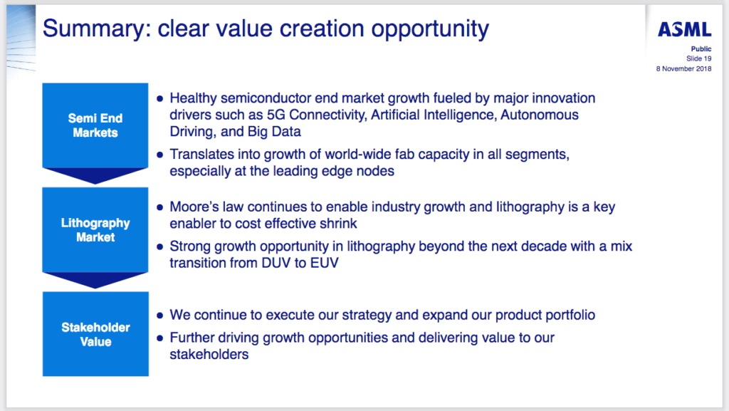
The above slide comes from ASML’s last investor day in 2018 and gives a general summary of where they are going. In the Q4 2020 results, which beat expectations for the quarter and the year, the finance director talked about the strong growth in sales of EUV systems but also referred to the next generation of High-NA EUV systems, which were expected to go into full production around 2025.
Below gives an idea of what High-NA is all about. “Moore’s law drives the doubling of the number of transistors per unit area every 2-3 years. To enable cost-effective shrink of future devices, a new High-NA EUV platform is being developed in a joint collaboration between ASML and Carl Zeiss SMT. The High-NA EUV scanner employs a novel Projection Optics Box (POB) design concept with a numerical aperture of 0.55 that enables 8nm half pitch resolution and a high throughput.”
You will be tested later on what that all means.
Meanwhile business is expanding strongly. “Good news for TSMC supplier ASML: the Taiwanese foundry will be increasing capital spending in 2021 to 25-28bn dollars, up from 17.2bn dollars last year. About 80pc of the capex is intended to build or expand advanced manufacturing capacity for 7nm, 5nm and 3nm. The bulk of it probably will go to 3nm, however, since that node is slated to move into volume production in the latter half of 2022.
My understanding of what is going on at ASML, which supplies the expensive machines that print the complex circuits on wafers created by companies like TSMC, is that the technology is moving from DUV (deep ultraviolet lithography) to EUV (extreme UV lithography) to High-NA (even more extreme UV lithography). They need to do this to deliver the capabilities that semiconductor makers need but it is at the extreme leading edge of technology and very hard to do, which is why ASML says they are still on the roadmap to producing High-NA EUV.
What is clear is that ASML is playing a critical role in overcoming a key bottleneck to the advancing technology revolution and management seem very confident that they can deliver what is needed.
“Total net sales for the year were €14.0bn, including €4.5bn from 31 EUV systems. For ASML, 2020 was a year of strong growth, both in sales and in profitability.
For 2021, we expect another year of growth driven by strong Logic demand and continued recovery in Memory. The build out of the digital infrastructure and the continued technology innovation is relevant to the consumer, automotive and industrial markets and drives demand across our entire product portfolio.”
The group is also intent on looking after shareholders. In addition to increasing the dividend by 15pc for 2020 the group announced a new €6bn (US$7.27bn) share buyback programme on top of the €12bn already spent on share buybacks.
Taiwan Semiconductor Manufacturing TSM Buy @ $130 MV: $681bn Employees: 48,752 Next figures: 22 April Times recommended: 3 First recommended: $95.5 Last recommended: $112.50
TSM is on a roll as evidenced by its sparkling 2020 results and massive cap ex plans for 2021.
“Taiwan Semiconductor Manufacturing Co. came through with an announcement of record capital spending: up to $28bn this year, a sum meant to extend its leadership as well as build the Arizona plant it intends to take care of certain American customers. The figure blows away its record last year of $17bn in spending and reflects not only confidence in the company’s growth but also an opportunistic move amid a surge in demand for semiconductors. Along with the massive spending plans, TSMC announced record revenues and profits. Net income jumped 23pc to NT$142.8bn – about $5.1bn, helping to build a 50pc increase in full-year profit. Revenues rose 14pc, to a record NT$361.5bn (about $12.9bn).”
The massive capex programme reflects industry fears of capacity shortages.
“The massive spending figure – more than half TSMC’s projected revenue for the year – may serve to alleviate industry concerns about a shortage, as demand (from areas including 5G smartphones and recovering auto sales) has strained industry production capacity. While phones have been crucial to TSMC’s business – the new iPhone was a key reason for the record Q4 revenues – its chairman says high-performance computing will crowd out smartphones to become the company’s leading growth driver.”
TSM is the king of the fab outsourcing business, one of a handful of companies shouldering the heavy burden of investing in the required foundry capacity so the chip design companies can focus on what they do best. One analyst looking at the company said “The company has a market cap near $500bn (now $681bn), but that’s minimal in relation to the next wave of technology. Fundamentally, the company manufactures chips for customers using 300 mm wafers at a variety of sizes, on the forefront of foundry technology.”
Demand appears to be insatiable. According to one analyst “Apple has already secured 80pc of TSM’s 2021 5nm production.“ In semiconductor manufacturing the 5nm process follows the 7nm node. In 2020, Samsung and TSMC entered volume production of 5nm chips, manufactured for companies including Apple, Marvell, Huawai and Qualcomm. The new chip coming along is 3nm
There’s more to being the provider of choice in a capacity limited industry where most supplier wafers are sold out than just selling wafers. Specifically, it’s important to pay attention to the fact that lower dimension (nm) wafers are capable of getting a much better selling price. From 16nm to 3nm the wafer price nearly triples.
At the just reported Q4 results, TSMC said it was expecting strong growth going forward and that would require high cap ex. “Today, as we enter another period of higher growth, we believe a higher level of capacity — capital intensity is appropriate to capture the future growth opportunities. We now expect a higher growth CAGR [compound annual growth rate] in the next few years, driven by the industry megatrends of 5G and HPC [high performance computing]-related applications.”
The company also noted. “As we enter the 5G era, a smarter and more intelligent world will require massive increases in computation power and greater need for energy-efficient computing, and therefore, require leading-edge technologies. Thus, HPC [high performance computing] is an increasingly important driver of TSMC’s long-term growth and the largest contributor in terms of our incremental revenue growth. With our technology leadership, we are well positioned to capture the growth from the favorable industry megatrend. We now expect our long-term revenue growth to be 10pc to 15pc CAGR from 2020 to 2025 in US dollar terms.”

You need advanced materials engineering and machines to work with wafers and chips (Applied Materials); you need massive investment in foundries and cutting edge technology to make wafers (Taiwan Semiconductor Manufacturing); you need high performance, unbelievably complex, lithography machines to print circuits on wafers (ASML); and you need to know that I studied PPE (politics, philosophy and economics) at university, not engineering so if I am making mistakes in my understanding of what all these companies do and how they do it I am not surprised and nor should you be.
The key point is not the detail of what these businesses are all about but the fact that the semiconductor industry is entering what is likely to be a sustained period of strong growth and these companies have a central role to play in what is happening.
They literally stand at the heart of the accelerating technology revolution.
This is why they are in the QV for Shares portfolio and why I expect them to prove rewarding investments over the next several years and probably the next decade.